Tesla's $25 Billion Terafab Gambit: Forging AI Independence and Redefining Vertical Integration
In a move poised to fundamentally reshape both the automotive and semiconductor landscapes, Tesla CEO Elon Musk has announced the imminent launch of t...
Editorial Team
World Of EV
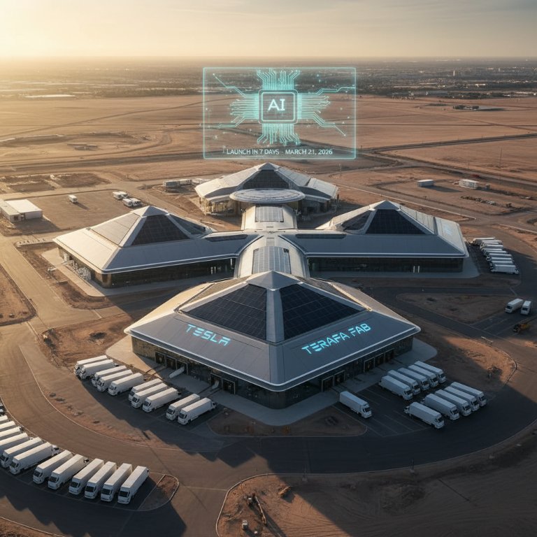
In a move poised to fundamentally reshape both the automotive and semiconductor landscapes, Tesla CEO Elon Musk has announced the imminent launch of the company's ambitious 'Terafab' project on March 21, 2026. This colossal initiative, a 'giga-sized AI chip manufacturing facility' as dubbed by Musk, represents a staggering approximately $25 billion investment and forms a critical pillar of Tesla's record capital expenditure plan for the year. The Terafab aims to bring the production of advanced artificial intelligence chips — including logic processing, memory storage, and advanced packaging — entirely in-house, directly addressing anticipated supply constraints that could otherwise hinder Tesla's aggressive AI roadmap.
For years, Tesla, like many tech giants, has relied on external foundries like TSMC and Samsung for the fabrication of its sophisticated chips, including its groundbreaking FSD processors. However, as the demands of advanced AI systems for autonomous driving, the Dojo supercomputer, and the Optimus humanoid robot escalate, this reliance has become a looming bottleneck. The Terafab project signals Tesla's emphatic shift towards complete vertical integration, a strategy that could provide unparalleled control over its most critical hardware and accelerate its technological advancements at a pace unmatched by competitors.
The Scale of Ambition: A $25 Billion AI Powerhouse
The Terafab is no ordinary manufacturing plant; it is designed to be 'way bigger' than Tesla's existing Gigafactories, positioning Tesla to become an integrated device manufacturer (IDM). This gigantic facility is engineered to produce an astounding 100 to 200 billion custom AI and memory chips per year. To put this into perspective, some reports suggest the facility could operate at over 100,000 wafer starts per month (WSPM), a scale that could rival some of the world's largest dedicated semiconductor manufacturers.
- Estimated Cost: Approximately $25 billion
- Components Produced: Logic processing, memory storage, and advanced packaging
- Annual Output Target: 100-200 billion custom AI and memory chips
- Strategic Purpose: Secure supply, enhance performance, and accelerate AI development for FSD, Dojo, and Optimus
Unpacking the 'AI5' and 2nm Frontier
At the heart of Terafab's mission is the production of Tesla's fifth-generation AI chip, the AI5. This advanced processor is targeting a bleeding-edge 2-nanometer (2nm) process technology. The 2nm node, while often a marketing term rather than a literal physical dimension, signifies a monumental leap in transistor density, speed, and power efficiency compared to previous generations. Only a handful of global semiconductor titans like TSMC and Samsung are currently at or approaching this level of sophistication in mass production, with TSMC having started volume production of its 2nm (N2) technology in Q4 2025. This move positions Tesla at the forefront of semiconductor manufacturing technology, aiming for a capability that very few companies in the world possess.
Why This Matters:
Tesla's Terafab project is far more than just a new factory; it's a profound strategic play with wide-ranging implications:
- Unrivaled Strategic Control & Supply Chain Resilience: The past few years have highlighted the fragility of global supply chains, particularly in semiconductors. By investing $25 billion into its own fabrication capabilities, Tesla gains unparalleled control over its most critical components. This eliminates reliance on external geopolitical factors or the capacity constraints of third-party foundries, ensuring a stable and secure pipeline for its rapidly expanding AI ambitions. This is a direct answer to Musk's previous warnings of hitting a 'chip wall' if external suppliers couldn't meet demand.
- Accelerated Innovation Velocity: Owning the entire chip design, manufacturing, and packaging process under one roof will drastically reduce iteration cycles. Tesla can design, test, and produce new AI chips with unprecedented speed, potentially giving it a significant lead in the race for advanced autonomous systems and robotics. This level of vertical integration is a powerful accelerator for innovation.
- Competitive Disruption and Market Signal: No other automotive manufacturer is undertaking chip fabrication at this scale. This move further distances Tesla from traditional automakers, solidifying its identity as a technology company first. It sends a clear signal to the market: Tesla is doubling down on AI as its core differentiator, and it will control every aspect necessary to dominate that space. This could pressure competitors to reconsider their own levels of vertical integration.
- Cost Efficiency and Long-Term Value: While the upfront $25 billion investment is colossal – comparable to or even exceeding the cost of many advanced fabs built by established players – it promises long-term cost efficiencies. By eliminating margins paid to external foundries and optimizing chip designs specifically for its needs, Tesla could significantly reduce the per-unit cost of its AI hardware over time. This investment, as part of a record capital expenditure, underscores a long-term vision for sustainable growth and profitability.
- A Risky, Yet Potentially Transformative, Bet: Building and operating a leading-edge semiconductor fab is notoriously complex, expensive, and requires highly specialized expertise. While Tesla has proven adept at manufacturing, chip fabrication is a different beast. However, if successful, Terafab could transform Tesla into a technology powerhouse on par with the likes of Intel or Samsung in terms of integrated capabilities, profoundly influencing the future of AI-driven mobility and beyond.
Conclusion:
Tesla's Terafab project marks a watershed moment in the company's evolution and a bold statement to the global technology industry. By committing a staggering $25 billion to achieve AI chip independence, Tesla is not merely building a factory; it is constructing the foundation for its next era of innovation and dominance. This audacious move promises to fortify its supply chain, accelerate its AI development, and cement its position as a technological vanguard, forcing both automotive and semiconductor incumbents to take note of a new, vertically integrated paradigm.